Invited Speakers
Area 1 Advanced CMOS: Material Science / Process Engineering / Device Technology
- 3D Stacked Devices and MOL Innovations for Post-Nanosheet CMOS Scaling Steven Demuynck (imec, Belgium)
- Gate Stack Engineering of Ferroelectric HfZrO2 from Multi-Level Non-Volatile Memory (NVM) to Analog-based Synapse Min-Hung Lee (National Taiwan Univ., Taiwan)
-
 Milli-Kelvin Analysis Revealing the Role of Band-edge States in Cryogenic
MOSFETs
Hiroshi Oka
(AIST, Japan)
- Realization of CMOS Operation in 3-Dimensional Stacked FET with Self-Aligned Direct Backside Contact Juhun Park (Samsung Electronics Co., Ltd., Korea)
Area 2 Advanced and Emerging Memories / New Applications
-
 HfO2-based Ferroelectric Capacitors for Non-Volatile Memory: Going from Single Devices to Memory Arrays
Ruben Alcala
(NaMLab, Germany)
- Online Training with Analog RRAM Chips Bin Gao (Tsinghua Univ., China)
- Metal Induced Lateral Crystallization (MILC) Techniques for Highly Scalable Vertical Si Channel in 3D Flash Memory Noritaka Ishihara (Kioxia Corporation, Japan)
-
Ferroelectric neuromorphic devices and system implementations
Thomas Kämpfe
(Fraunhofer Institute for Photonic Microsystems, Germany) -
 Materials Development and Interfacial Engineering for Emerging Ferroelectric
Memories
Min Hyuk Park
(Seoul National Univ., Korea)
Area 3 Heterogeneous and 3D Integration / Interconnect / MEMS
-
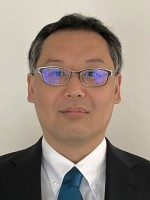 Evaluation Platforms for Next-Generation Semiconductor Packaging Technologies
Hirokazu Noma
(Resonac Corp., Japan)
-
 MEMS Activities at AIST: Ultrathin Piezoelectric MEMS
Yusuke Takei
(AIST, Japan)
- Area Selective Deposition to Facilitate Integration Christophe Vallee (SUNY Albany/TEL, USA)
-
 Backside Power Delivery Process Integration Challenges
Liesbeth Witters
(imec, Belgium)
Area 4 Power / High‐speed Devices and Materials
- High Power and High Frequency Diamond Field Effect Transistors Hiroshi Kawarada (Waseda Univ., Japan)
-
Grating Gate GaN/AlGaN Plasmonic FETs for THz Optoelectronics Devices
Wojciech Knap
(Warsaw Univ. of Technology and Polish Academy of Sciences, Poland) - Engineering of Channel Mobility and Threshold Voltage in AlSiO/AlN/p-type GaN Metal–Oxide–Semiconductor Field-Effect Transistors Tetsuo Narita (Toyota Central R&D Labs., Japan)
-
 Comprehensive Research on Nitrided SiO2/4H-SiC Interfaces
Heiji Watanabe
(Osaka Univ., Japan)
-
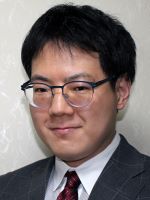 Ultra-high Voltage SiC Bipolar Devices for Green Infrastructure
Naoki Watanabe
(Hitachi, Ltd., Japan)
- Pairing Ga2O3 with p-NiO produces robust power diodes for harsh environments Jiandong Ye (Nanjing Univ., China)
Area 5 Photonics: Devices / Integration / Related Technology
-
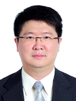 Optical Coatings for Metamaterials and Metasurfaces
Yi-Jun Jen
(National Taipei Univ. of Technology, Taiwan)
-
 Heterogeneously Integrated Membrane Lasers on Si and Thin-film lithium niobate
Platforms
Yoshiho Maeda
(NTT Device Technology Labs., Japan)
- High-Frequency Dynamics in Silicon Photonic Modulators Wei Shi (Laval Univ., Canada)
Area 6 Energy Harvesting and Converting Devices and Materials
-
 Development of functional thin-film materials for Si solar cells and their
application to perovskite/Si tandems
Takuya Matsui
(AIST, Japan)
-
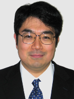 Key issues for developing high performance thermoelectric materials and
devices
Takao Mori
(NIMS, Japan)
-
 Prospects of PV recycling in Germany
Andreas Obst
(Fraunhofer CSP, Germany)
Area 7 Organic / Molecular / Bio‐electronics
- Molecular design of organic thermoelectric materials: From precise doping to device functionalization Chong-an Di (ICCAS, China)
-
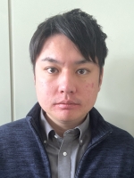 Fabrication of single-molecule electret memory devices based on Fe-FET
Architecture
Masaru Fujibayashi
(National Institute of Technology, Ube College, Japan)
-
 Emissions from persistent charge carriers in organic semiconductors
Ryota Kabe
(OIST, Japan)
- Semiconductor Physics of Lead Halide Perovskites Yoshihiko Kanemitsu (Kyoto Univ., Japan)
-
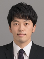 Highly deformable semiconductor devices using stretchable conjugated polymer
materials
Naoji Matsuhisa
(The Univ. of Tokyo, Japan)
Area 8 Low Dimensional Devices and Materials
-
 MX2 Layer transfer: A path towards integrating epitaxial 2D materials in a
300mm pilot line
Souvik Ghosh
(imec, Belgium)
-
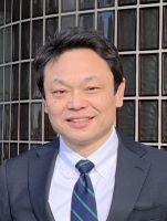 Photonic III-V semiconductor nanowires on Si toward wafer scale
functionalization
Fumitaro Ishikawa
(Hokkaido Univ., Japan)
- Modulation of 2D semiconductors by chemical procedures Daisuke Kiriya (The Univ. of Tokyo, Japan)
-
 The Growth of N-polar AlN for Electronic Applications
Markus Pristovsek
(Nagoya Univ., Japan)
- Optimization and Localization of Molecular-Beam-Epitaxy-grown GaAs-based Quantum Dots Andreas Dirk Wieck (Ruhr-Universität Bochum, Germany)
Area 9 Novel Functional / Quantum / Spintronic Devices and Materials
- 2D lead-tin halides for energy-efficient neuromorphic electronic devices Maria Loi Antonietta (Univ. of Groningen, Netherland)
-
 From spin-orbitronics to orbitronics: efficient manipulation of topological
spin structures for memory and unconventional computing
Mathias Kläui
(Johannes Gutenberg-Universität Mainz, Germany)
- New material-based approaches in quantum devices Tomohiro Otsuka (Tohoku Univ., Japan)
Area 10 Thin Film Electronics: Oxide / Non‐single Crystalline / Novel Process
- Low temperature poly-Ge TFTs on glass and plastic substrates Akito Hara (Tohoku Gakuin Univ., Japan)
- Recent advances in oxide-TFT technology for next-generation sustainable electronics Kenji Nomura (UC San Diego, USA)
-
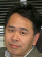 High Mobility Thin film Transistors for Three Dimensional LSIs fabricated by
ALD process
Yukiharu Uraoka
(NAIST, Japan)
Area 11 Advanced Materials: Synthesis / Crystal Growth / Characterization
-
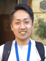 Laser-based photoemission electron microscopy as a nondestructive imaging tool
for ferroelectric devices
Hirokazu Fujiwara
(The Univ. of Tokyo, Japan)
- High pressure synthesis of boron nitride and diamond single crystals and their impurity control Takashi Taniguchi (NIMS, Japan)
-
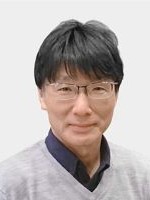 Metrology informatics on semiconductor ~ Multimodal analysis of gallium nitride as examples ~
Shigetaka Tomiya
(NAIST, Japan)
- High-precision 3D integration of catalytic silicon nanowires for high performance electronics Linwei Yu (Nanjing Univ., China)
-
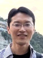 Three-Level Charge Pumping Technique for SiC-MOS Interface Characterization
Hiroshi Yano
(Univ. of Tsukuba, Japan)
Area 12 Advanced Circuits / Systems Interacting with Innovative Devices and Materials
Invited Speakers
- Area 1 Advanced CMOS: Material Science / Process Engineering / Device Technology
- Area 2 Advanced and Emerging Memories / New Applications
- Area 3 Heterogeneous and 3D Integration / Interconnect / MEMS
- Area 4 Power / High‐speed Devices and Materials
- Area 5 Photonics: Devices / Integration / Related Technology
- Area 6 Energy Harvesting and Converting Devices and Materials
- Area 7 Organic / Molecular / Bio‐electronics
- Area 8 Low Dimensional Devices and Materials
- Area 9 Novel Functional / Quantum / Spintronic Devices and Materials
- Area 10 Thin Film Electronics: Oxide / Non‐single Crystalline / Novel Process
- Advanced Materials: Synthesis / Crystal Growth / Characterization
- Area 12 Advanced Circuits / Systems Interacting with Innovative Devices and Materials
