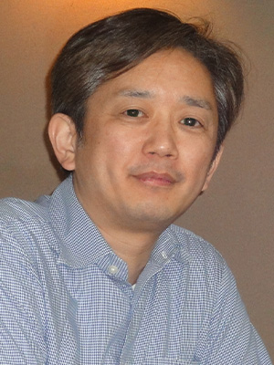
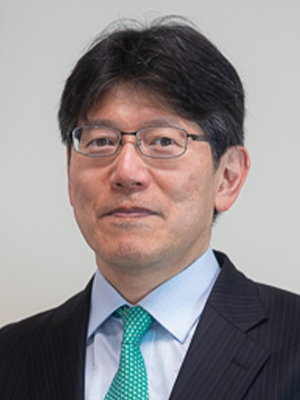
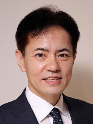
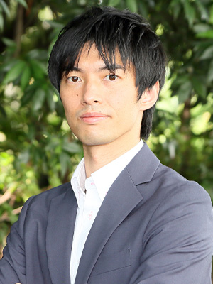
Tuesday, September 5, 2023 [Short Course A] Leading-edge CMOS Technology for 2nm-node and beyond (Room F (224), Bldg. 2)[Short Course B] Plasma technology: Cornerstone of the post-scaling and next milestone of assurance energy and environment (Room K (234), Bldg. 2)
A
Leading-edge CMOS Technology for 2nm-node and beyond
Organizer:
Meishoku Masahara (AIST)
Chair: Toshifumi Irisawa (AIST)
13:00 – 13:45
“Logic Scaling Trend”
Yuzo Fukuzaki
(Rapidus US, Formerly with TechInsights)
13:45 – 14:30
“Chip Design Democratization for Scaled CMOS”
Makoto Ikeda
(Univ. of Tokyo)
14:30 – 15:15
“Advanced Technologies for Extending EUV Lithography”
Seiji Nagahara
(Tokyo Electron Ltd.)
15:15 – 15:30
Break (15 min)
15:30 – 16:15
“Fundamental Insights into Advanced Processes of 3D
Integration”
Fumihiro Inoue
(Yokohama National Univ.)
16:15 – 17:00
“2D FETs with TMDC films for CFET and 3DI Transistors”
Hitoshi Wakabayashi
(Tokyo Tech)
17:00 – 17:45
“Complimentary FET process technology towards functional scaling”
Tatsuro Maeda
(AIST)
B
Plasma technology: Cornerstone of the post-scaling and next milestone of assurance energy and
environment
Organizer:
Kenji Ishikawa (Nagoya Univ.)
Chair: Masanori Terahara (Western Digital Corp.)
13:00 – 13:45
“CMOS+X for functional diversification of post-scaling
microelectronics”
Andreas Mai
(IHP)
13:45 – 14:30
“Sustainable CMOS Scaling in Nanosheet Era”
Naoto Horiguchi
(imec)
14:30 – 15:15
“Dry Etching Technology for Logic Device”
Masaru Izawa
(Hitachi High-Tech Corp.)
15:15 – 15:30
Break (15 min)
15:30 – 16:15
“Technological direction of high aspect ratio etching for
memory devices”
Akihiro Tsuji
(Tokyo Electron Ltd.)
16:15 – 17:00
“Prospect of dry etching technology for 3D・Chiplet integration”