Awards
SSDM Award
The SSDM Award is awarded to researchers who contributed an outstanding paper at the past SSDM conferences.
High Voltage Bipolar‐Mode MOSFET with High Current Capability
The Insulated Gate Bipolar Transistor (IGBT) is currently the leading power semiconductor device. During initial development, however, the IGBT had an intrinsic problem. Latch‐up phenomena, which were caused by the thyristor structure inherent in the device, narrowly limited the Safe Operating Area (SOA) for voltage and current. This paper proposed and demonstrated the first tangible solution in the world to this problem. The concept became the theoretical guideline for designing IGBTs commercialized in countries around the world. It can be said that this paper was the starting point for such practical implementation.
Around 1980, research was actively being pursued on the MOS‐controlled thyristor which an MOS gate turns on and off, to be the power semiconductor that would globally succeed the high‐voltage bipolar transistor. Among those efforts, the discovery that a horizontal MOS thyristor could operate the transistor (1978) prompted greater interest in development of a device structure that would realize the operation. However, these attempts were unable to solve the problem of the thyristor easily latching up on account of the PNPN structure with its alternating P‐type and N‐type layer arrangement, which was essentially inherent in the device structure. As such, no practically applicable device ever resulted. Amid the focus of much research on the flow of electrons, this paper showed that it was possible to formulate conditions triggering latch‐up by focusing on the hole current supplied by P‐type layer on the back surface of the chip and that, based on this, a design which would prevent latch‐up could be worked out. The outcome of this paper was that the SOA of the IGBT expanded significantly up to a practical level, opening the way for commercialization as well as developing rapidly on high power IGBTs for industrial motors and other applications.
Currently, the IGBT has been developed to handle even higher current densities (for home appliances) and its high performance has been realized at overwhelmingly low cost. This has made it a core device in fields applying power semiconductors. It has also been projected the IGBT will be a key device in CO2 reduction and renewable energy adoption. The IGBT market continues to grow 10% annually and could conceivably reach 1 trillion yen.
As explained above, the results of the research published in this paper have made a substantial contribution from a fundamental perspective to the development of industrial applications for the IGBT, the most important power device of our day, and the paper's great contribution has also been acknowledged from the standpoint of constructing device design guidelines that fully utilize numerical simulations. Therefore, the SSDM Award is presented to the authors of this paper in recognition of their achievements.
-
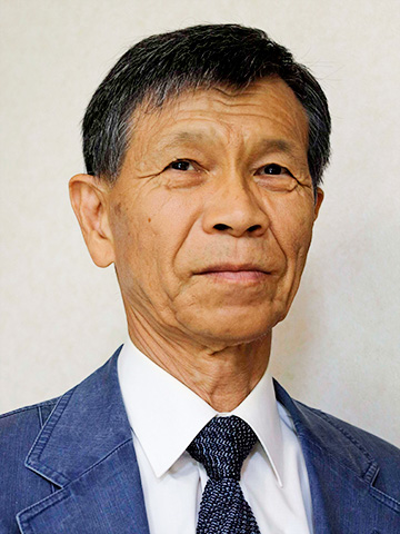
Akio Nakagawa
Nakagawa Consulting Office, LLCAkio Nakagawa received the B.Sc. and M.Sc. degrees in physics in 1972 and 1974, and the Ph.D. degree in electrical engineering in 1984, all from Tokyo University. In 1974, he joined Toshiba R&D Center, where he was engaged in the development of various power devices. In 1984, he developed world first non‐latch‐up IGBTs. From 1981 to 1983, he was a visiting scholar in the Electrical & Computer Engineering Dept. of the Univ. of Mass., Amherst. He published over 150 technical papers. He received Okochi Memorial Technology Prize in 1990 and IEEE William E. Newell Power Electronics Award in 2010, all for development of non‐latch‐up IGBTs, and received ISPSD Award in 1998 for his paper of high voltage SOI technology. He was granted over 190 U.S. patents and over 100 Japanese patents. He retired from Toshiba Corp. in 2009, and is currently President of Nakagawa Consulting Office, LLC. Dr. Nakagawa is a life senior member of IEEE, and a fellow member of IEE Japan.
-
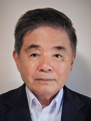
Hiromichi Ohashi
Corporation Aggregates, NPERC‐J (Next generation power electronics and system research consortium Japan)He received M.S. degree in electronics from Sophia university in 1969 and Ph. D degree from Tohoku University in 1990. From 1969 to 2002, he joined Research and Development Center, Toshiba Corporation, Kawasaki Japan. After being involved in sensor system development for Artificial‐satellite, he engaged in research activities for a novel power device and Its application technologies. From 2002 to 2004, he was a professor of the Tokyo Institute of Technology. From 2003 to 2013, he was working for the Power electronics Center of AIST as an invited researcher. From 2014 to 2019, he was director of the Green Electronics Research Center of City Kitakyushu. From 2014, he has been president of the NPERC‐J. He was General Chairman of the 1995 ISPSD (International Symposium on Power Semiconductor Devices and ICs). In 1999, He received the Purple Ribbon Award from Japan Government.
-
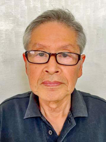
Tsuneo Tsukakoshi
Tsuneo Tsukakoshi Joined Toshiba Central Research Laboratory (former Toshiba Research & Development Center) in 1965. In 1968, he engaged in the development of compact color imaging tubes. Since 1973, engaged in the development of power semiconductor devices such as 600V 100A GTO, high voltage power MOSFETs, 6000V 2500A Light Triggered Thyristor, and high voltage IGBTs. In 2002, he retired from Toshiba Research & Development Center. In 1997, he received Oyama Matsujiro Award for his contribution to the development and commercialization of IGBTs.
SSDM Paper Award (PA)
SSDM Paper Award is awarded to the best paper presented at the previous year's SSDM.
2 Department of Electrical and Electronic Engineering, Tokyo Institute of Technology, Japan
3 Tokyo Tech Academy for Super Smart Society, Tokyo Institute of Technology, Japan
-
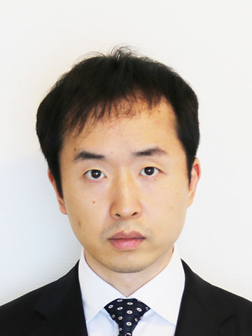
Noriyuki Lee
Hitachi, LtdDr. Noriyuki Lee is a researcher at the Center for Exploratory Research, Hitachi, Ltd., Japan. He graduated and received his PhD degree in applied physics from the University of Tokyo in 2011. At the University of Tokyo, he conducted experimental research concerning on quantum optics and quantum information science. Since 2011, he has been with Hitachi, Ltd. and is engaged in research on quantum computing using silicon quantum dots.
-
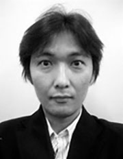
Ryuta Tsuchiya
Hitachi, Ltd.Ryuta Tsuchiya received the B.S., M.S., and Ph.D. degrees in material science from the Tokyo Institute of Technology, Tokyo, Japan, in 1993, 1995, and 1998, respectively.
Since 1998, he joined the Central Research Laboratory (CRL), Hitachi, Ltd., Tokyo, Japan, where he has been engaged in the research and development of high‐speed and low‐power CMOS devices, including thin‐film SOI and BOX transistors until 2008. From 2008 to 2013, he has been working on the research and development of energy conversion devices such as SiC MOSFETs and high‐efficiency photovoltaic cells.
From 2013 to 2016, he was a deputy laboratory manager of Hitachi Cambridge Laboratory, UK. Currently, he is a Chief Researcher with Research and Development Group, Hitachi, Ltd. His current research interests include quantum information processing based on Si‐based manufacturing process. -
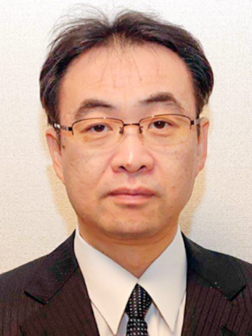
Yusuke Kanno
Hitachi, Ltd.Yusuke Kanno received the B.S. and M.S. degrees in physics from Tohoku University, in 1992 and 1995, respectively. He received Ph.D. degree from Tokyo Institute of Technology in 2009. He joined the Central Research Laboratory, Hitachi, Ltd. in 1997, where he has been engaged in the research and development of high‐speed and low‐power circuits for embedded DRAMs and microprocessors. He was engaged in the establishment of the power gating technology for mobile SoCs. From 2010, he managed the research team of the high‐speed and power‐saving circuit technique for information and telecommunication system. From 2012, he engaged in high reliable system by using SRAM‐based FPGA for industrial business. From 2019, he joined quantum computing project in the Center for Exploratory Research. He is a member of the IEEE Solid‐State Circuit Society.
-
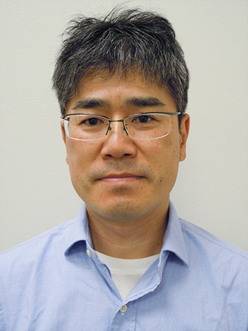
Toshiyuki Mine
Hitachi, Ltd.Toshiyuki Mine graduated from Nagasaki Technical High School, Nagasaki, Japan, in 1982. He joined he Central Research Laboratory, Hitachi Ltd. in 1982 and was been engaged in the research and development of CVD technology. From 2019, he has been engaged in research on quantum computing using silicon quantum dots.
-
Yoshitaka Sasago
Hitachi, Ltd.Yoshitaka Sasago received his Bachelor's, Master's and Doctor's degrees in applied physics at the University of Tokyo, Japan. After he joined Hitachi, Ltd., Tokyo, Japan, he developed DRAM capacitor technologies and flash memory technologies. He contributed to the R&D and the mass production of AG‐AND‐type flash memory chips. After that, he has been engaged in the emerging fields of the semiconductor technologies including a brain‐neocortex device, a cross‐point phase‐change memory, a chain‐cell‐type phase‐change memory, an FET‐type gas sensors and a solid oxide fuel cell. His research results are summarized at the Google Scholar profile: https://scholar.google.es/citations?user=7hu6K6EAAAAJ&hl=en
-
Go Shinkai
-
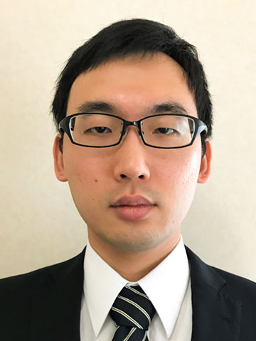
Raisei Mizokuchi
Tokyo Institute of TechnologyRaisei Mizokuchi was born in Tokyo, Japan, in 1989. He received the B.Eng. and M.Eng. degrees in physical electronics from Tokyo Institute of Technology, Japan, in 2012 and 2014, respectively. In 2018, he received a doctoral degree in physics from Université Grenoble Alpes, France, where he studied germanium low‐dimensional devices. He also received another doctoral degree in physical electronics from Tokyo Institute of Technology, Japan, in 2021. During the degree, he worked on the characterization silicon quantum dot devices and the development of techniques for spin qubit readout. Currently, he is a researcher at Tokyo Institute of Technology and has been continuously working on the development of spin readout techniques.
-
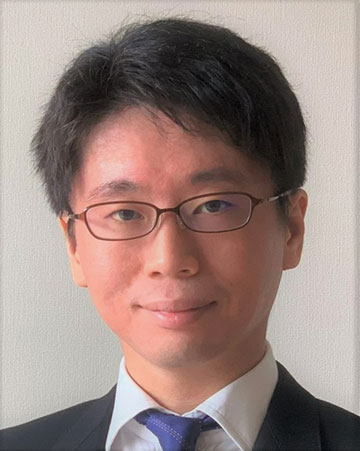
Jun Yoneda
Tokyo Institute of TechnologyJun Yoneda is a Specially Appointed Associate Professor at Tokyo Tech Academy for Super Smart Society, Tokyo Institute of Technology. He received his B.Eng., M.Eng., and D. Eng. degrees from the University of Tokyo, in 2009, 2011, and 2014, respectively. From 2011 to 2014, he was a recipient of Research Fellowship for Young Scientists (DC1) from Japan Society for the Promotion of Science (JSPS). He conducted research at RIKEN, Japan, and the University of New South Wales, Australia, before joining Tokyo Institute of Technology, Japan, in 2020. He was also a PRESTO researcher at Japan Science and Technology Agency from 2021 to 2022. He was a recipient of 25th Marubun Research Encouragement Award (2021) and the 2021 Suematsu Award “Fundamentals and Developments of Digital Technology”. His research interests include semiconductor qubits, spin manipulation, silicon quantum computers, and quantum nanoscience.
-

Tetsuo Kodera
Tokyo Institute of TechnologyTetsuo Kodera received his B. S., M. S., and Ph. D in Physics from the University of Tokyo, in 2002, 2004, and 2007, respectively. He is an Associate Professor at the Department of Electrical and Electronic Engineering, Tokyo Institute of Technology. His research interests include quantum technology, solid state physics, and fundamental technology for quantum computing devices. He has published more than 80 papers in reputed journals. He was the recipient of the Presentation Award of the Japan Society of Applied Physics, and The Young Scientists' Prize of The Commendation for Science and Technology by the Minister of Education, Culture, Sports, Science and Technology.
-
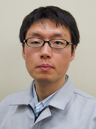
Chihiro Yoshimura
Hitachi, Ltd.Chihiro Yoshimura received a B.A. degree in environmental information and an M.A. degree in media and governance from Keio University, Kanagawa, Japan, in 2005 and 2007, respectively. In 2007, he joined the Central Research Laboratory, Hitachi Ltd., Tokyo, Japan, where he has been engaged in research and development on supercomputers and mission‐critical servers, including vector processors, interconnect switches, and network controllers. He received the 33rd Advanced Technology Award (Fuji Sankei Business i Prize) in 2019 for his contributions to domain‐specific computer architecture solving large scale optimization problem. Since 2020, he has been engaged in research on quantum computer. Currently, he is a Project Leader and Chief Researcher in the Center for Exploratory Research, Research and Development Group, Hitachi Ltd. He served on the Designers' Forum Committees of the ASP‐DAC 2021. He currently serves as a board member of the IPSJ SIG on system architecture. He is also a doctoral student at the Tokyo Institute of Technology, Tokyo, Japan.
-
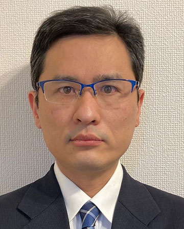
Shinichi Saito
Hitachi, Ltd.Shinichi Saito completed his Ph.D. in theoretical condensed‐matter physics at Waseda University in 2000. Then, he joined Hitachi in Japan, and developed CMOS front‐end process and device technologies. He developed a model for the mobility reduction in an MOSFET with high‐k gate stacks, and won the SSDM Best Paper Award in 2003. He also won his 2nd SSDM best paper award (2011) for the stimulated emissions from Si fin light‐emitting diode. He published 266 papers, including 53 invited talks. He also filed 21 patents and made 10 press releases. In 2012, he moved from his senior research position in Hitachi to the school of Electronics and Computer Science in the University of Southampton taking up a professorship. Saito has wide range of interdisciplinary research background on physics, nano‐electronics, and Si photonics with strong industrial experience. In 2020, he went back to Hitachi for quantum computing.
-
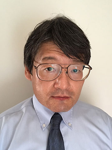
Digh Hisamoto
Hitachi, Ltd.Digh Hisamoto received the B.S., M.S. and Ph.D. degree from the University of Tokyo in 1984, 1986, and 2003, respectively.
In 1986, he joined Central Research Laboratory, Hitachi, Ltd., Tokyo, where he has been working on ULSI device physics and process technologies. He developed scaled CMOS including FinFET, memory devices, RF devices, MONOS devices, Si photonics, tunnel devices and SiC power devices. From 1997 to 1998, he was a Visiting Industrial Fellow at University of California, Berkeley. From 2015 to 2019, he was invited as a Visiting Professor at Tokyo Institute of Technology, where he started the research of quantum sensors and quantum computing devices.
He has served as a conference committee member of IEDM, VLSI Symposium and SSDM, and an Associate Editor of IEEE Electron Device Letters. He also served as Executive Director of Japan Society of Applied Physics (JSAP).
Dr. Hisamoto is a Fellow of JSAP and IEEE. -
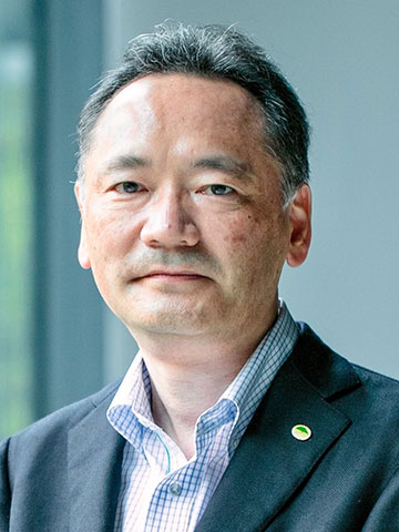
Hiroyuki Mizuno
Hitachi, Ltd.Hiroyuki Mizuno received the B.S., M.S., and Dr.Eng. degrees in electronic engineering from Osaka University, Osaka, Japan, in 1991, 1993, and 2001, respectively. In 1993 he joined the Central Research Laboratory, Hitachi, Ltd., Tokyo, Japan where he has been engaged in the research and development of high‐speed and low‐power semiconductor circuits for SRAMs, microprocessors (SuperH), system‐on‐a‐chip (SH‐Mobile). He is also a pioneer in quantum‐inspired computers (CMOS Annealing Machine). From 2002 to 2003 he was a visiting scholar at the Department of Computer Science, Stanford University, Stanford, CA. He is currently a distinguished researcher in the Center for Exploratory Research (CER), and the laboratory manager of the Hitachi‐Kyoto University Laboratory at Hitachi. From 2020 he is the project manager of the “Large‐Scale Silicon Quantum Computer Project,” one of the moonshot R&D programs launched by the Japanese Cabinet Office (CAO). His current research interests include silicon quantum computing, artificial‐intelligence systems using cognitive neuroscientific methods, and cyber‐human systems. He is a Fellow of IEEE, and also a member of ACM.
SSDM Young Researcher Award (YRA)
SSDM Young Researcher Award is awarded to the first authors of excellent papers presented at the previous year's SSDM. Authors who are 33 years old or younger as of April 1st of the year following the conference in which the paper was presented are eligible for the award.
Computing‐in‐Memory Demonstration of Multiple‐State (>8) Analog Memory Cell with Ultra‐Low (<1 nA/cell) Current Enabled by Monolithic CCAC‐IGZO FET +Si CMOS FET Stack for Highly‐Efficient AI Applications
-

Satoru Ohshita
Semiconductor Energy Laboratory Co., Ltd.Satoru Ohshita was born in Hyogo, Japan, in 1992.
He received the B.S. degree in electrical and electronic engineering from Kindai University, Osaka, Japan, in 2015. In 2015, he joined Semiconductor Energy Laboratory Co., Ltd., Atsugi, Japan.
His recent interests include characteristics of oxide‐semiconductor FETs, high performance edge AI device based on Analog in‐memory computing.
A Novel 1T2R Self‐Reference Physically Unclonable Function Suitable for Advanced Logic Nodes for High Security Level Applications
-

Yu‐Hsuan Lin
Macronix International Co., Ltd.Yu‐Hsuan Lin received the Ph.D degree in electronics engineering from National Chiao Tung University, Taiwan, in 2020.
She joined the Emerging Central Laboratory in Macronix International since 2014. Her research interest includes resistive random access memory, conductive bridging random access memory, phase change memory, and Flash memory. Her research works cover the device characterization, reliability and physical simulation. She also focuses on nonvolatile memory based neuromorphic computing, in‐memory‐computing, and in‐memory‐searching. She publishes 29 international journal and conference papers, and 15 US patents.
“Regrowth‐free” Fabrication of AlGaN/GaN HBT with N‐p‐n Configuration
-

Takeru Kumabe
Nagoya UniversityMr. Takeru Kumabe is a Ph.D. candidate and Japan Society for the Promotion of Science research fellow DC1 at the Department of Electronics, Nagoya University, Japan. He received his master's and bachelor's degrees from the Department of Electronics, Nagoya University in 2019 and 2021, respectively, under the supervision of Prof. Yoshio Honda and Prof. Hiroshi Amano. His research interests include the design, crystal growth, fabrication, and characterization of gallium nitride (GaN)‐based high‐power/high‐frequency devices. In particular, he currently works on developing crystal growth and fabrication technologies for GaN‐based heterojunction bipolar transistors to apply in next‐generation communication technologies.
Lasing from a valley photonic crystal ring resonator with a bearded interface
-
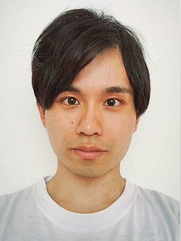
Ryosuke Miyazaki
Recruit Co., Ltd.I was originally born in Kochi prefecture and raised until the age of 18. I majored in electronic engineering in Osaka university and belonged to Kondo laboratory. we studied on fabrications and optical characteristics of a photonic crystal resonator with a sub‐resonator. After graduation from it, I became a member of Iwamoto laboratory in University of Tokyo as a Master's student. we studied on a valley photonic crystal resonator with a bearded interface. We fabricated the ring resonator on an InGaAsP slab containing multiple quantum wells as a gain material. We performed micro‐photoluminescence measurements at low temperature and confirmed lasing oscillation using a cavity mode originating from a topological edge state at the interface. We were awarded the excellent Master's thesis award this past March. Now, I work in Recruit Co., Ltd. as a product designer of Air‐wait.
Charge/Discharge Reactions via LiPON/Multilayer‐Graphene Interfaces without Li+ Desolvation/Solvation Processes
-
Satoshi Yamamoto
Nagoya UniversityI received bachelor's and master's degrees from Nagoya University in 2020 and 2022, respectively. I am now a doctor course student of Nagoya University. My research interest is related to reactions at the interface between carbon anode and solid electrolyte.
For the further spread of electric vehicles, it is essential to improve the performance of batteries. High‐rate charging is a particularly challenging issue. I believe that the results presented here will provide clues to solving this issue. I currently investigate the effects of carbon anode and solid electrolyte factors on charging and discharging, respectively.
By continuing to work on this research theme, I would like to clarify what elements are required for high‐rate charging/discharging at the interface between carbon anode and solid electrolyte.
Universal Method on Charge Carrier Mobility and Series Resistance Extraction in Two‐Dimensional Field‐Effect Transistors
-

Yu‐Chieh Chien
National University of SingaporeYu‐Chieh Chien is currently pursuing his Ph.D. degree with the Department of Electrical and Computer Engineering, National University of Singapore (NUS), Singapore. His current research topic includes two‐dimensional semiconductors and ferroelectric memories with the focus on their device physics and process integrations. He received his B.S. degree with the Department of Materials and Optoelectronic Science, National Sun Yat‐Sen University (NSYSU), Taiwan, in 2018.
Prior to his Ph.D. study, he was an international scholar at the Department of Large Area Electronics, Imec, Belgium and the KU Leuven, Belgium, where he was working on parameter extractions and bias temperature instability issues for amorphous oxide semiconductors.
He was the recipient of the 2018 IEEE Electron Device Society Masters Student Fellowship Award for the demonstration of significant ability to perform research in the fields of electron devices during his undergraduate study.
Room‐temperature spin injection and spin‐to‐charge conversion in a ferromagnetic semiconductor / topological insulator heterostructure
-
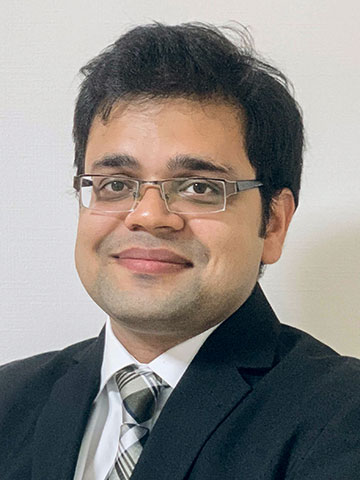
Shobhit Goel
1 Department of Electrical Engineering and Information Systems, The University of Tokyo, 7‐3‐1 Hongo, Bunkyo‐ku, Tokyo 113‐8656, Japan.
2 CREST, Japan Science and Technology Agency, 4‐1‐8 Honcho, Kawaguchi, Saitama 332‐0012, Japan.Shobhit Goel received his B.Tech. degree in Electronics and Communication Engineering from the Indian Institute of Information Technology, Jabalpur, India in 2013, Master's degree in Advanced Material Physics and Engineering from the National Physical Laboratory (CSIR‐NPL), India in 2015, and Ph.D. degree in Electrical Engineering from the University of Tokyo, Japan in 2019 under the supervision of Prof. Masaaki Tanaka. His Ph.D. dissertation primarily focuses on a study of the magnetic anisotropy (MA) of novel ferromagnetic semiconductor (FMS) (Ga,Fe)Sb expected to be used in Spintronics applications. After his Ph.D., he joined University of Tokyo as a project researcher in CREST, Japan Science and Technology sponsored project, with the aim to develop room‐temperature device applications based on Fe‐doped III‐V ferromagnetic semiconductors. Since January 2022, he has been working as a Central Process Integration Engineer in the Micron Memory, Hiroshima, Japan, where he works for the development and manufacturing of DRAM memory.
High mobility hydrogenated indium oxide thin‐film transistors (InOx:H TFTs) formed by low‐temperature solid phase crystallization
-
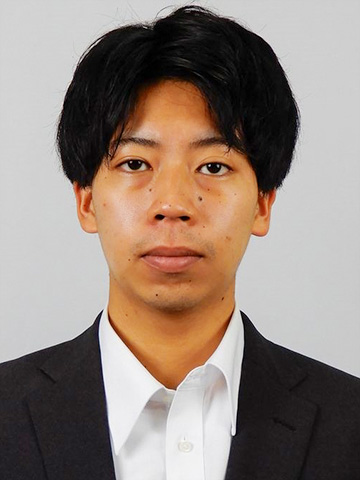
Taiki Kataoka
Kochi University of Technology, JapanTaiki Kataoka received B.E. and M. E. degrees in Environmental Science and Engineering from Kochi University of Technology, Japan, in 2020 and 2022, respectively. During his master course, he worked on the research of polycrystalline indium oxide thin film for thin‐film transistor application.
First demonstration of photoresponsivity in a polycrystalline Ge‐based thin film
-
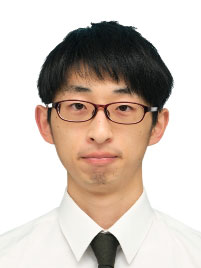
Takuto Mizoguchi
University of TsukubaTakuto Mizoguchi was born in Ibaraki, Japan, in 1998.
He received the B.E. and M.E. degrees of semiconductor engineering from University of Tsukuba under the guidance of Associate Professor Kaoru Toko, in 2020 and 2022, respectively.
His research interests were low‐temperature synthesis of polycrystalline group 4 alloy thin films and demonstrated photoresponsivity in polycrystalline Ge thin films for the first time.
After completing the M.E. program, he joined Sony Semiconductor Solutions, Ltd. In 2022 and have been engaged in research and development of image sensors.
Call for 2022 SSDM Award Nomination
The SSDM Award was established to recognize outstanding contributions to academic or industrial development in the field of solid state devices and materials.
Papers to be nominated for the 2022 SSDM Award should be among those that have been presented between the 1st SSD conference in 1969 and the 48th SSDM conference in 2016.
The SSDM Award will ultimately be decided by the SSDM Organizing Committee after a recommendation is made by the SSDM Award Nomination Committee.
The recommendation will be in accordance with the following two criteria.
-
1) Originality
The award‐winning selection must be original, and must have had significant theoretical or practical impact in the field of solid state devices and materials.
-
2) Contribution
The author(s) of the award‐winning selection must have played or be playing a pioneering or leading role, with globally outstanding contributions in the technological field.
Candidate and Nominator Eligibility
-
– Candidates Eligible for the Award
All authors who presented papers between the 1st SSD conference in 1969 and the 48th SSDM conference in 2016, excluding papers written by this year's Organizing Committee Chair and Award Nomination Committee Chair.
-
– Persons Eligible for Nominating Candidates
Anyone, excluding this year's members of the SSDM Award Nomination Committee
Submission Process for SSDM Award Nominations
The following is the process for submitting nominations.
- – Before deciding on a candidate for the award, confirm the eligibility of nominators and candidates once again.
-
– Download the Nomination Form.
[ SSDM Award Nomination Form (MS‐Word) ] -
– Fill out the Nomination Form and send it to the SSDM Secretariat by the nomination deadline.
The deadline for nomination has been extended to May 29, 2022. CLOSED
If you have any questions, please ask the secretariat by e‐mail
Sumitomo‐shoji Kanda‐Izumi‐cho Bldg., 12F,
1‐13 Kanda‐Izumi‐cho Chiyoda‐ku Tokyo, Japan 101‐0024


