

Award
There are three categories of awards for authors who presented papers at the SSDM:
the SSDM Award, the SSDM Paper Award, and the SSDM Young Researcher Award.
SSDM Award
The SSDM Award will be will be awarded to researchers who contributed an outstanding paper at past SSDM. The Award Committee selects this award.
NTT LSI Laboratories
In this paper, how the world's top-level high-frequency characteristics were achieved through the development of a lattice-matched InAlAs/InGaAs high-electron-mobility transistor (HEMT) on an InP substrate with a T-shaped gate was described. The design guidelines based on systematic investigations of the short-channel device structure were also presented.
In the early 1990s when this paper was published, the InAlAs/InGaAs HEMT on an InP substrate was expected to become a key device in 40 Gbps optical communications systems or millimeter-wave wireless communications. This is because it had promising high-speed/high-frequency characteristics that surpassed those of Si or GaAs devices. Thus, to improve these characteristics, the scaling down of the device was intensively studied. It was reported that the high-frequency characteristics required for a 40 Gbps optical communications system could be achieved by using a pseudomorphic InAlAs/InGaAs HEMT on an InP substrate with a gate length reduced by 0.05 µm. However, the breakdown voltage of this pseudomorphic HEMT was low. Therefore, the application of the device was severely limited, and it was difficult to apply it to the logic circuits of 40 Gbps optical communications systems.
In this paper, the fabrication of lattice-matched InAlAs/InGaAs HEMTs on an InP substrate with excellent breakdown voltage characteristics and gate lengths of 0.5 to 0.05 µm, and the systematic investigation of the immunity to the short-channel effect with respect to the design of the channel layer and the barrier layer were reported. Consequently, the use of a lattice-matched HEMT with a gate length of 0.05 µm was found to result in a current gain cutoff frequency of 300 GHz and a maximum oscillation frequency of 235 GHz, which are comparable to those of pseudomorphic HEMTs.
Since the device technology reported in this paper demonstrated that both breakdown voltage and high-frequency characteristics can be attained simultaneously, it has been used as a basic technology of integrated circuits for optical communications and opened the door to the practical application of 40 Gbps optical communications.
On the basis of the above, the great contribution of this paper to industry and academia is recognized. We here present this SSDM Award in honor of its value.
-
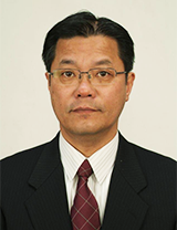
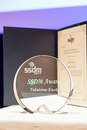
Takatomo Enoki
NTT Electronics CorporationTakatomo Enoki received M.S. degrees in physics and Dr. Eng. degree in electrical engineering from the Tokyo Institute of Technology in 1984 and 1996, respectively.
In 1984, he joined the Atsugi Electrical Communications Laboratories of NTT. Since then, he has been engaged in R&D on fabrication technologies for high-frequency and high-speed integration circuits using compound semiconductors for optical and wireless communications systems.
After serving as a director of Photonics Laboratories at NTT, he moved to NTT Electronics Corp. as a senior vice president of the broadband system & device business group in 2012 and is developing compound semiconductor devices for communications systems.
He is a fellow of the IEEE and the IEICE. -
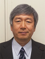
Yohtaro Umeda
Tokyo University of ScienceYohtaro Umeda received the B.S. and M.S. degrees in physics and the Ph.D. degree in electrical engineering from the University of Tokyo, Tokyo, Japan, in 1982, 1984, and 2000, respectively. In 1984, he joined Nippon Telegraph and Telephone (NTT) Corporation and engaged in high-speed circuit application of GaAs MESFETs and InP HEMTs. He moved to Tokyo University of Science, Chiba, Japan, as a professor, where he is engaged in the study of high-speed analog/digital circuits and signal processing for radio and optical communication systems. He is a member of the JSAP, IEICE, and IEEE.
-

Yasunobu Ishii
ISHII P.E.Jp OfficeYasunobu Ishii was born in Fukuoka Prefecture, Japan, on 19 June, 1950. He received the B.E., M.E., and D.E. degrees in electronics from Osaka University, Japan, in 1973, 1975, and 1984, respectively. In 1975, he joined the Electrical Communication Laboratories, NTT, Tokyo, Japan, where he has been engaged in research on GaAs FETs and ICs. From 1983 to 2000,he was with NTT Atsugi Laboratories where he conducted research on InP-based heterostructure electron devices. In 2001, he joined NTT Electronics Corp., to establish 6” GaAs IC production line. In 2003 he resigned from NTT group, and joined Yokowo Co., ltd., where he has engaged in millimeter-wave devices for the automotive radars. From 2014, he has engaged in engineering consultant at ISHII P.E.Jp Office in Yokohama as a certificated Professional Engineer of Japan.
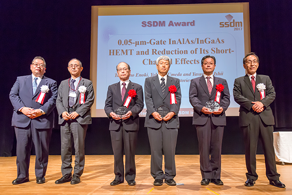
T. Endoh (Chair), K. Shiraishi (Chair), Y. Ishii, Y. Umeda, T. Enoki and H. Ohno (Chair)
History of the SSDM Award is hereSSDM Paper Award
SSDM Paper Award2017 will be awarded to the best paper presented at SSDM2016.
1.Univ. Grenoble Alpes, CEA, LETI, MINATEC Campus(France), 2.STMicroelectronics(France), 3.Univ. de Lyon(France)
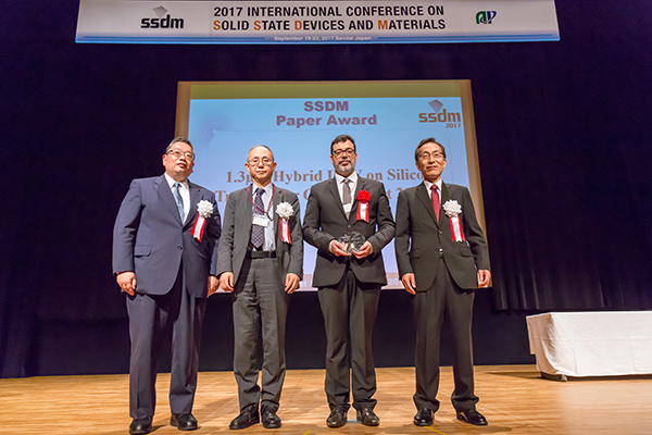
T. Endoh (Chair), K. Shiraishi (Chair), F. Boeuf and H. Ohno (Chair)
History of the SSDM Paper Award is hereSSDM Young Researcher Award
SSDM Young Researcher Award 2017 will be awarded to outstanding papers authored by young researchers and presented at SSDM2016.
1.Graduate School of Engineering, Nagoya University, 2.Institute of Materials and Systems for Sustainability, Nagoya University, 3.JST-CREST, 4.Hitachi, Ltd., Research & Development Group, Center for Technology Innovation-Electronics.
1.CEA-LETI(France), 2.CEA-LIST(France), 3.Inserm(France)
1.Univ. of Tokyo(Japan), 2.PROVIGATE Inc.(Japan)
1.Kyushu Univ.(Japan)
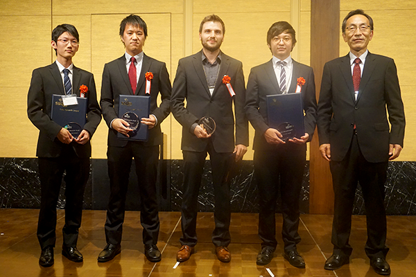
M. Ishitaki, S. Nishitani, T. Werner, H. Shirakawa and H. Ohno (Chair)
History of the SSDM Young Researcher Award is hereCall for 2017 SSDM Award Nomination
The SSDM Award was established to recognize outstanding contributions to academic or industrial development in the field of solid state devices and materials.
Papers to be nominated for the 2017 SSDM Award should be among those that have been presented between the 1st SSD conference in 1969 and the 43rd SSDM conference in 2011.
The SSDM Award will ultimately be decided by the SSDM Organizing Committee after a recommendation is made by the SSDM Award Nomination Committee.
The recommendation will be in accordance with the following two criteria.
-
1) Originality
The award-winning selection must be original, and must have had significant theoretical or practical impact in the field of solid state devices and materials.
-
2) Contribution
The author(s) of the award-winning selection must have played or be playing a pioneering or leading role, with globally outstanding contributions in the technological field.
Candidate and Nominator Eligibility
-
- Candidates Eligible for the Award
All authors who presented papers between the 1st SSD conference in 1969 and the 43rd SSDM conference in 2011, excluding papers written by this year’s Organizing Committee Chair and Award Nomination Committee Chair.
-
- Persons Eligible for Nominating Candidates
Anyone, excluding this year’s members of the SSDM Award Nomination Committee
Notice: Self-nominations are permitted beginning last year. In the case of self-nomination, at least one endorsement letter (any form is acceptable) from persons other than the authors of the paper must be submitted along with the Nomination Form.
Submission Process for SSDM Award Nominations
The following is the process for submitting nominations.
- - Before deciding on a candidate for the award, confirm the eligibility of nominators and candidates once again.
- - Download the Nomination Form
Download the Nomination Form (MS-Word). - - Fill out the Nomination Form and send it to the SSDM Secretariat by the nomination deadline.
Nomination deadline: March 27, 2017 Closed
If you have any questions, please ask the secretariat by e-mail
Sumitomo-Shoji Kanda-Izumi-cho Bldg., 13F
1-13 Kanda-Izumi-cho, Chiyoda-ku, Tokyo 101-0024
closed on March 27